- High throughput, large area FIB processing up to 1 mm
- Ga-free microsample preparation
- Ultra-high resolution, field-free FEG-SEM imaging and analysis
- In-lens SE and BSE detection
- Resolution optimization for high-throughput, multi-modal FIB-SEM tomography
- Superior field of view for easy navigation
- Essence™ easy-to-use, modular graphical user interface
-

-
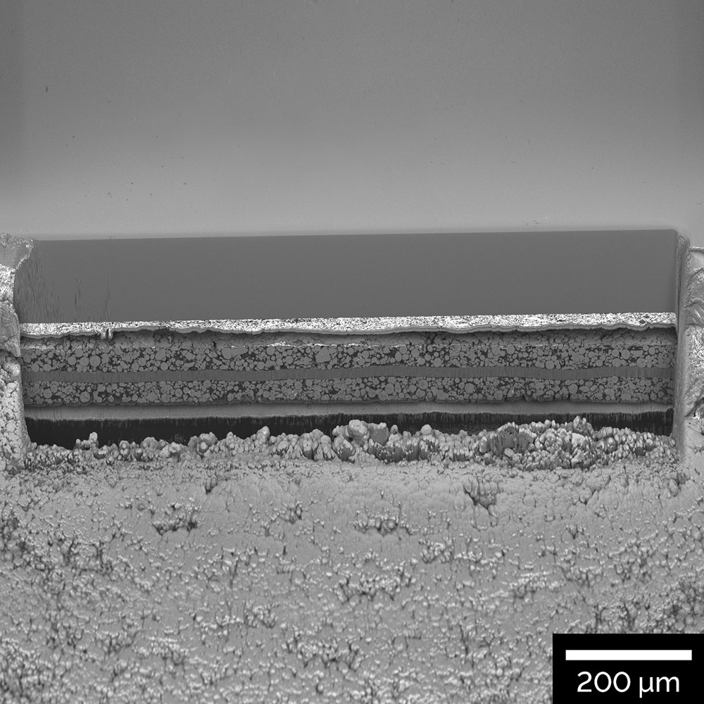
1 mm wide polished cross section of a Li-ion battery electrode
-

-
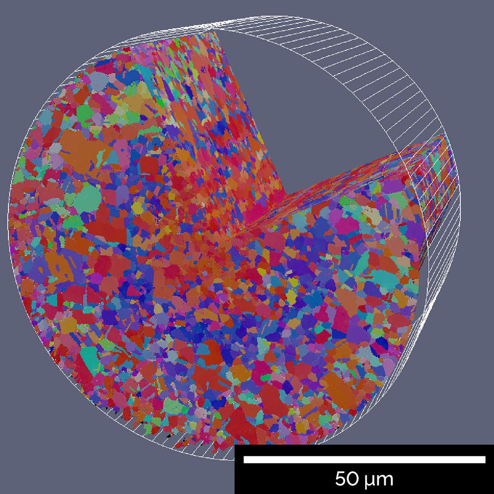
EBSD map of a 90 µm diameter cold-drawn copper wire
-

-
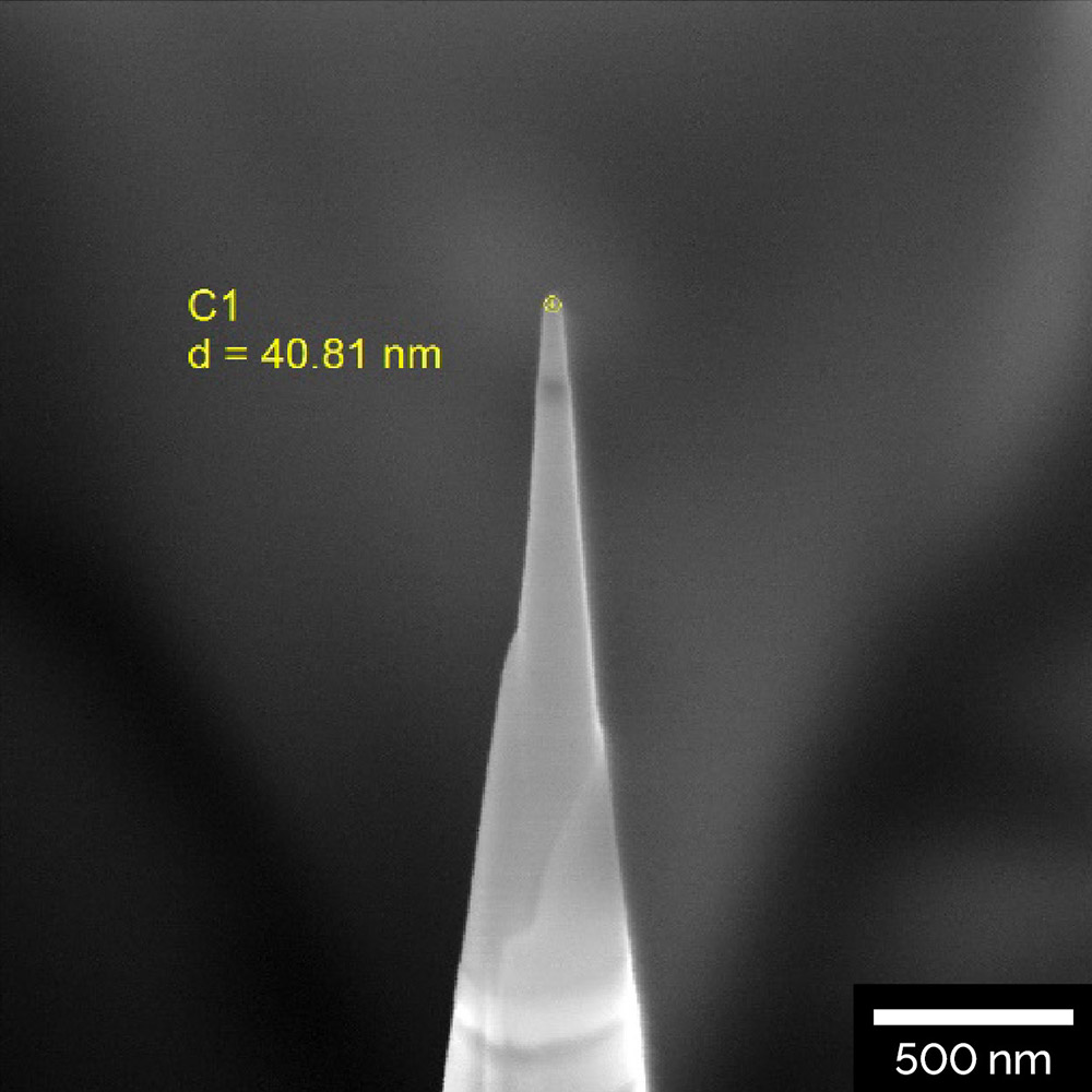
Ga-free atom probe tip sample preparation using plasma FIB
Webinar Recording
Take your multi-modal materials characterization further with our latest plasma FIB-SEM
WATCH NOW
The link above will get you to our webinar recording at GoToWebinar platform.